
Here is an article for anyone that is curious about FPGA core development and would like some help getting started. You can access the full article by clicking here. Below are a few points that are covered.
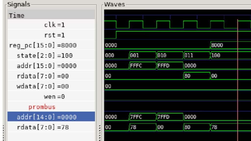
- The goal is to build a basic version of the Family Computer (Famicom/NES) CPU (Central Processing Unit).
- The original Famicom CPU is based on the famous MOS Technology 6502 chip.
- This project only implements a minimal set of 11 commands needed to run a simple “Hello World” program.
- The hardware design is written in a language called Veryl, which describes electronic circuits.
- This design is intended for use with an FPGA (a programmable chip) in the future.
- The core components created include the CPU, RAM (temporary memory), ROM (program memory), and a Bus (the communication system).
- A tool called Verilator is used to run a simulation of the hardware on a computer, instead of using a physical chip.
- The simulated system is designed to load a small “Hello World” program.
- Because the graphics chip (PPU) is not implemented, the program cannot display text.
- Success is confirmed by checking the CPU’s internal log to prove it correctly executed the required steps and instructions.
Small but important note: the article is in Japanese, but that’s not an insurmountable problem for non-native speakers anymore 🙂